Your connection to advanced PCB manufacturing
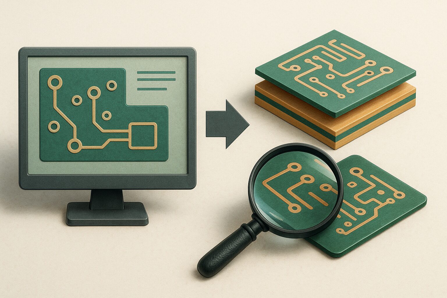
Vias are critical to achieving high interconnect density, especially in HDI designs. Summit uses microvias, blind and buried vias, and via-in-pad structures to route complex circuits within tight spaces. These features reduce signal path length, improve electrical performance, and allow for higher component density without increasing layer count.
PCB Manufacturing
Frequently asked PCB manufacturing and assembly questions
Rigid and HDI PCBs
-
-
The annular ring is the copper pad area surrounding a drilled hole, and maintaining precise dimensions is essential for electrical and mechanical reliability. Summit’s laser and mechanical drilling processes, combined with tight registration control, ensure annular ring integrity in accordance with IPC-6012 Class 3 requirements, even on microvia and fine-pitch designs.
-
HDI PCBs support higher signal speeds by shortening trace lengths, reducing parasitic inductance, and enabling controlled impedance routing. This is critical for high-frequency and high-speed digital designs used in computing, telecommunications, and advanced electronics.
-
Building an HDI PCB often requires multiple sequential lamination cycles, laser drilling, copper filling, planarization, and precise imaging for fine-line features. Each step must be tightly controlled to maintain dimensional accuracy and electrical performance, especially for mission-critical applications.
-
We follow lean manufacturing principles, minimize scrap through precise process control, and use IPC standards to reduce rework and waste. By optimizing yields on complex builds, Summit supports both operational efficiency and environmental responsibility.
About Summit

News