Our software-driven facilities deliver comprehensive printed circuit board manufacturing solutions for every application, from rapid prototype PCBs to high-density interconnect (HDI) boards with advanced via structures.
Need a Custom PCB Solution? Our engineering team can provide expert design for manufacturability (DFM) support to optimize your PCB layout before production.
Backdrilling is a cost-effective method to improve signal integrity without adding costly additional sub-lamination structures. This process removes the unneeded portion of a via barrel that can cause signal reflections at high speed data rates, or on high frequency RF designs.
Board Details
Standard
Advanced
Emerging
Layer Count
2-30
32+
>48
Minimum panel size
12″ x 18″
Maximum panel size
18″ x 24″
21″ x 24″
24″ x 30″
HDI layers
2 – 3
4
8+ as permitted by laminate type
Sequential laminations
2 – 3
4
8+ as permitted by laminate type
Layer-to-layer registration
+/- .002″
Thickness
Design and manufacturing factors usually determine the thickness of PCBs.
Thickness
Standard
Advanced
Emerging
Minimum board thickness, single/double sided
.005″
002
Maximum board thickness
.250″
.300″
Minimum core thickness
.001″
.0005″
Minimum core thickness (BC, Kapton)
.002″
.001″
.0005″
Minimum prepreg fill
.003″
.002″
<.002″
Drill and Mill
PCB drilling and milling creates holes, slots, and other cavities in an electronic circuit board.
Drill and Mill
Standard
Advanced
Emerging
Minimum drill diameter, mechanical drill
.006″
.005″
.004″
Mechanical drill aspect ratio, unfilled
12:01
15:01
30:1
Mechanical drill aspect ratio, filled
10:01
11:01
> 11:1
Drill to metal (rigid)
.008″
.007″
.00525″
Drill to metal (flex)
.012″
.007″
.00525″
Drill edge to rigid flex transition
.100″
.075″
< .050″
Antipad diameter over drill size
.020″ +
.016″
< .050″
Minimum class 2 annular ring, mechanical drill
.005″
.004″
<.004″
Minimum class 3 annular ring, mechanical drill
.007″
.006″
<.006″
Minimum drill diameter, laser micro via
.004″
.003″
<.003″
Microvia aspect ratio
0.6:1
0.7:1
>0.7:1
Microvia capture pad / hole
+.007″
+.005″
+.004″
Control depth drill tolerance
Keep back .010″ +/- .005″
Keep back .005″ +/- .002″
Keep back .004 +/- .0015″
Back drill, diameter over primary drill
.008″
.007″
<.007″
Back drill anti-pad, diameter over primary drill
.016″
.014″
<.014″
Etch Features
Copper is one of the most important elements in printed circuit boards. The current carrying capacity of a PCB depends on the thickness of the copper trace.
Copper traces are made by using chemicals to etch or remove copper from the board except where the wired connections are present.
Etch Features
Standard
Advanced
Emerging
Minimum copper foil – internal
1/2 oz.
1/4 oz.
1/4 oz.
Maximum copper foil – internal
2 oz.
4 oz.
6 oz
Minimum copper foil – external
3/8 oz.
1/4 oz.
1/4 oz
Maximum copper foil – external
1 oz.
3 oz.
>3 oz
Inner and External Layers Print and Etch
Trace width and spacing requirements are based on the functionality of the circuit. They can affect electrical performance and signal integrity.
Inner Layers
Standard
Advanced
Emerging
Minimum designed line width/spacing, 1/4 ounce foil
.002″
<.002″
Minimum designed line width/spacing, 3/8 ounce foil
.003″/.003″
.0025″/.003″
<.0025″/.002″
Minimum designed line width/spacing, 1/2 ounce foil
.004″/.004″
.003″/.003″
<.0025″/.002″
Minimum designed line width/spacing, 1 ounce foil
.005″/.005″
.004″/.004″
.0035″/.004″
Minimum designed line width/spacing, 2 ounce foil
.008″/.008″
.006″/.008″
.006″/.006″
Minimum designed line width/spacing, 3 ounce foil
.010″/.010″
.008″/.010″
.008″/.008″
Plated External Layers
Standard
Advanced
Emerging
Minimum designed line width/spacing, 1/4 ounce foil
.0025″/.0025″
.002″/.002″
Minimum designed line width/spacing, 3/8 ounce foil
.004″/.004″
.003″/.003″
.0025″/.003″
Minimum designed line width/spacing, 1/2 ounce foil
.005″/.005″
.004″/.004″
.003″/.004″
Minimum designed line width/spacing, 1 ounce foil
.006″/.006″
.005″/.005″
.004″/.005″
Minimum designed line width/spacing, 2 ounce foil
.012″/.012″
.010″/.010″
.008″/.008″
Copper fill to round feature spacing (donuts)
.006″
.005″
.005″
Soldermask
Soldermask is a thin layer of polymer that protects PCBs from oxidation and corrosion. It also helps avoid solder bridges and gives color to the board.
Soldermask
Standard
Advanced
Emerging
LDI solder mask minimum web width, green color
.004″
.003″
less than .003″
LDI solder mask clearance
+/-.002″
+/-.0015″
less than +/- .0015″
Legend
With more PCBs moving towards high-density, flex, and component miniaturization, the quality and readability of a legend is more important than ever.
Legend
Standard
Advanced
Emerging
Inkjet legend printing
White
White
White
Color options
Green
Red, Blue, Black, White
Red, Blue, Black, White
Mechanical
Mechanical
Standard
Advanced
Emerging
Board profile dimensional tolerance
+/- .005″
+/- .002″
<+/- .002″
Plated through hole diameter tolerance
+/-.003″
+/-.002″
<+/- .002″
Non-plated through hole diameter tolerance
+.002″/ -.001″
+/-.001″
<+/- .001″
Flatness, warp and twist Per IPC-TM-650 2.4.22
<.75%
<.5% Balanced Construction
Unbalanced Constructions AABUS
Impedance Testing
Impedance Testing
Standard
Advanced
Emerging
Impedance controlled – single ended +/- %
+/- 10%
+/- 5%
<+/- 2%
Impedance controlled – edge couped diff. +/- %
+/- 10%
+/- 8%
<+/- 5%
Impedance controlled – broad side diff. +/- %
+/- 10%
+/- 8%
+/- 5%
Electroplating
The electroplating process deposits metal onto the surface of the circuit board and inside the plated through-holes. The most common plated metal is copper.
Electroplating
Standard
Advanced
Low Stress Nickel
100 Microinches
250 Microinches
Gold Plating Thickness
30 Microinches
As Specified
Hole Aspect Ratio
12 to 1
20 to 1
Finishes
The finish of a board, which is sometimes overlooked, is the interface between the board and the components that make the board function as desired.
Finishes
Standard
Advanced
HASL & HASL PB FREE
Yes
Yes
White Tin
Yes
Yes
Electroless Nickel/Palladium/Gold -ENEPIG
Yes
Yes
Electroless Nickel/Immersion Gold – ENIG
Yes
Yes
Immersion Silver
Yes
Yes
Entek Plus HT/OSP
Yes
Yes
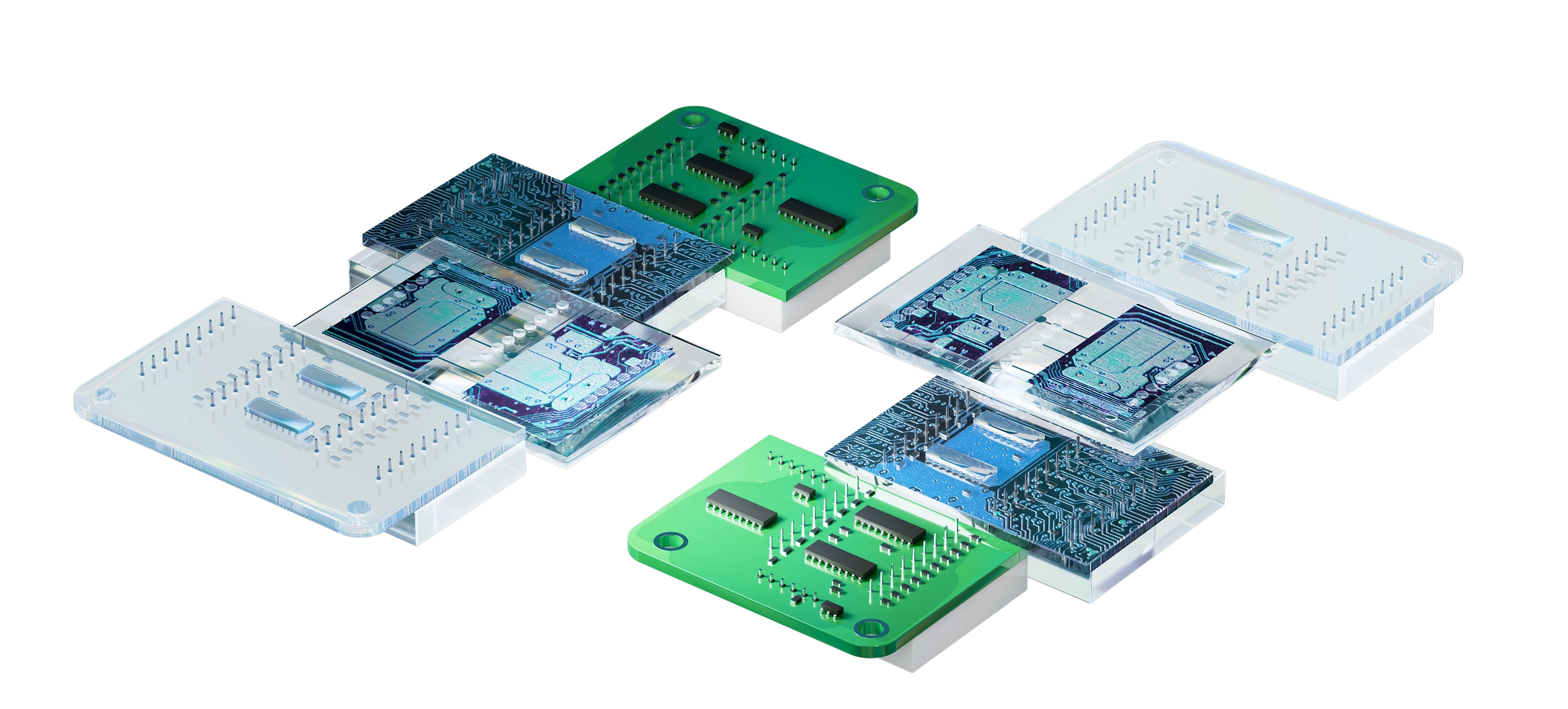
Vias
Vias make electrical connections between layers on a printed circuit board. They can carry signals or power between layers. Summit specializes in advanced PCB technologies such as blind vias, buried vias, and via-in-pads.
Types of Vias
Standard
Advanced
Laser Micro Vias
.006″
<.006″
Blind / Buried Vias
.006″
< .006″
Via in Pad
Yes
Yes
Via Fill
Standard
Advanced
Non-Conductive ViaFill
Yes
Yes
Silver / Conductive Epoxy Via Fill
No
Yes
Copper Filled Vias
No
Yes
Through Hole Copper Filled Via
No
Max 20 mils
Inspection Processes and Options
Thorough testing and inspection occurs throughout the production process to ensure problems are captured early on, ensuring high quality and yield.
Summit can fabricate PCBs ranging from simple 2-layer boards to highly complex designs with 30+ layers as standard, and emerging capabilities extend beyond 44 layers.
Standard maximum panel size is 18″ x 24″, with advanced capabilities up to 21″ x 24″ and emerging capabilities reaching 24″ x 36″.
Yes, Summit offers HDI layers and sequential laminations from 2-3 up to 7 layers as permitted by laminate type.
Summit specializes in advanced PCB technologies including laser micro vias, blind vias, buried vias, and via-in-pad, with options for non-conductive, conductive epoxy, and copper-filled vias.
Summit offers HASL (leaded and lead-free), White Tin, ENEPIG, ENIG, Immersion Silver, and Entek Plus HT/OSP finishes for both standard and advanced applications.
Yes, Summit provides full turnkey PCB assembly including single and double-sided SMT, through-hole assembly, BGA placement, and additional services like box build, conformal coating, and functional testing.
Summit Interconnect maintains comprehensive quality certifications including AS9100D, IPC Class II and III, ITAR registration, and RoHS compliance. Certifications vary by facility based on specialized capabilities.
View our certifications by facility or contact us to match your project with the right certified location.
For inner layers with 1/2 oz. copper, Summit can achieve .003″/.003″ trace width/spacing in advanced capabilities, with emerging capabilities below .0025″/.002″.
MSIRobot
Celebrating 10 Years of Summit Interconnect
Summit Interconnect is celebrating 10 years of trusted PCB manufacturing and the partnerships that have made it possible.
 Your connection to advanced PCB manufacturing