Icon about-block-ico-1 Icon about-block-ico-2 Icon about-block-ico-3 Icon about-block-ico-4 Icon announcement-close Icon arrow-left Icon arrow-right Icon arrow-sm Icon asterisk Icon banner-transparent-vector Icon btn-callback-ico Icon careers-item-location Icon careers-item-time Icon careers-item-type Icon careers-mail-ico Icon careers-phone-ico Icon careers-search-ico Icon careers-single-hero-vector Icon careers-single-more-vector Icon careers-vector Icon check Icon close Icon dfm-image-left-vector Icon dfm-image-right-vector Icon document Icon download-popup-vector Icon dropdown Icon envelope Icon facebook Icon faq-banner-bg Icon faq-title-ico-active Icon faq-title-ico Icon featured-links-block-bg Icon figure-1 Icon figure-10 Icon figure-11 Icon figure-12 Icon figure-13 Icon figure-14 Icon figure-15 Icon figure-2 Icon figure-3 Icon figure-4 Icon figure-5 Icon figure-6 Icon figure-7 Icon figure-8 Icon figure-9 Icon file-upload Icon form-sidebar-back Icon form-step-done Icon gmap-marker-group-icon Icon gmap-marker-icon Icon header-profile-ico Icon instagram Icon link Icon linkedin Icon loader Icon mail Icon phone Icon play-yt Icon play Icon post-nav-arr-left Icon quote-banner-vector Icon quote-block-aside-vector Icon quote-contact-phone-ico Icon quote-contact-position-ico Icon sidebar-location Icon sidebar-phone Icon technology-banner-nav-left-vector Icon technology-banner-nav-right-vector Icon twitter Icon webinar-item-date-vector Icon whitepaper-img-ico-left Icon whitepaper-img-ico-right Icon whitepapers-listing-banner-ico Icon whitepapers-single-aside-vector Icon youtube Icon yt-play-button
header-top-card Your connection to advanced PCB manufacturing
Download a brochure

    Panelized Board Size

    Due to our advanced operational capacity and nearly limitless flexibility, we can assemble more PCBs faster than anyone else in the industry.

    Board DetailsStandardAdvanced
    Board Size.25″ x .25″ minimum size, panelized17″ x 21″

    Processes

    Our assembly facility utilizes the latest technology and equipment, and we always keep tabs on industry trends and customer demand to make sure our capabilities meet your PCBA needs.

    Assembly ProcessesStandardAdvanced
    3, 5, and 10-Day TurnsYesYes
    Single-Sided SMTYesYes
    Double-Sided SMTYesYes
    Through HoleYesYes
    No CleanYesYes
    Clean / WashYesYes
    ROHS and LeadedYesYes
    Additional Assembly ProcessesStandardAdvanced
    Press FitsYesYes
    Box BuildYesYes
    Fine Pitch to 08 Mils.08 Mils.04 Mils
    BGA Repair and ReballYesYes
    Part Removal and ReplacementYesYes
    UnderfillNoYes
    StakingNoYes
    Conformal CoatingNoYes
    Fencing and ShieldsNoYes

    Components

    We provide full turnkey PCB assembly and manufacturing to help our customers across the country complete their projects on time. Our close and authentic partnerships with the most reputable US-based component and board suppliers is at the heart of the process. Test

    ComponentsStandardAdvanced
    SOICYesYes
    QFPYesYes
    TQFNYesYes
    LeadlessYesYes
    Through HoleYesYes
    LGAYesYes
    PassivesDown to 0201Down to 01005
    BGAs, uBGA, and VFBGAYesYes
    Leadless Chip Carriers/ CSPYesYes
    MicroelescronicsYesYes
    Package-on-PackageYesYes
    Flip ChipsYesYes
    HardwareNoYes
    Component PackagingStandardAdvanced
    Cut TapeYesYes
    Loose PartsYesYes
    ReelsYesYes

    Soldering Types & Methods

    Soldering is one of the most basic techniques to understand for PCB assembly. Serving as a connective and conductive glue, a solid solder brings continuity and functionality to any circuit board.

    Soldering OptionsStandardAdvanced
    Jet Paste PrintingYesYes
    Stencil/Water Soluble PasteNoYes
    Vapor Phase ReflowNoYes
    Conventional ReflowYesYes
    Wave Solder / Selective SolderYesYes
    Programmable Selective SolderNoYes

    Inspection & Testing

    Inspection is a critical part of the PCB assembly process. Without it, electronics manufacturers would never know for sure whether the PCB—and therefore the device—would work properly.

    Inspection ProcessesStandardAdvanced
    Flying ProbeNoYes
    3D BGA X-RayYesYes
    Functional TestingNoYes
    In-Line AOIYesYes
    Visual InspectionYesYes
    Component InspectionYesYes
    Component Value CheckYesYes
    Ionic Contamination TestNoYes

    Quality Standards

    Following quality standards ensures all aspects of a PCB design are correctly implemented and the end products perform exactly as expected.

    Quality StandardsStandardAdvanced
    AS9100DYesYes
    AS9102 FAIRNoYes
    IPC Class IIYesYes
    IPC Class IIINoYes
    ITAR CertifiedYesYes
    RoHS CompliantYesYes

    Depanelization Methods

    Once the boards are assembled and tested, they will need to be separated into their individual parts. There are many methods of depaneling PCBs, and which one you use depends on the type of panelization you chose.

    Depanelization MethodsStandardAdvanced
    V-ScoreYesYes
    Mouse BitesYesYes
    Mechanical RoutingNoYes

    Manufacturing Capabilities Overview

    Download Summit’s Capabilities
    FAQ

    Frequently Asked Questions:

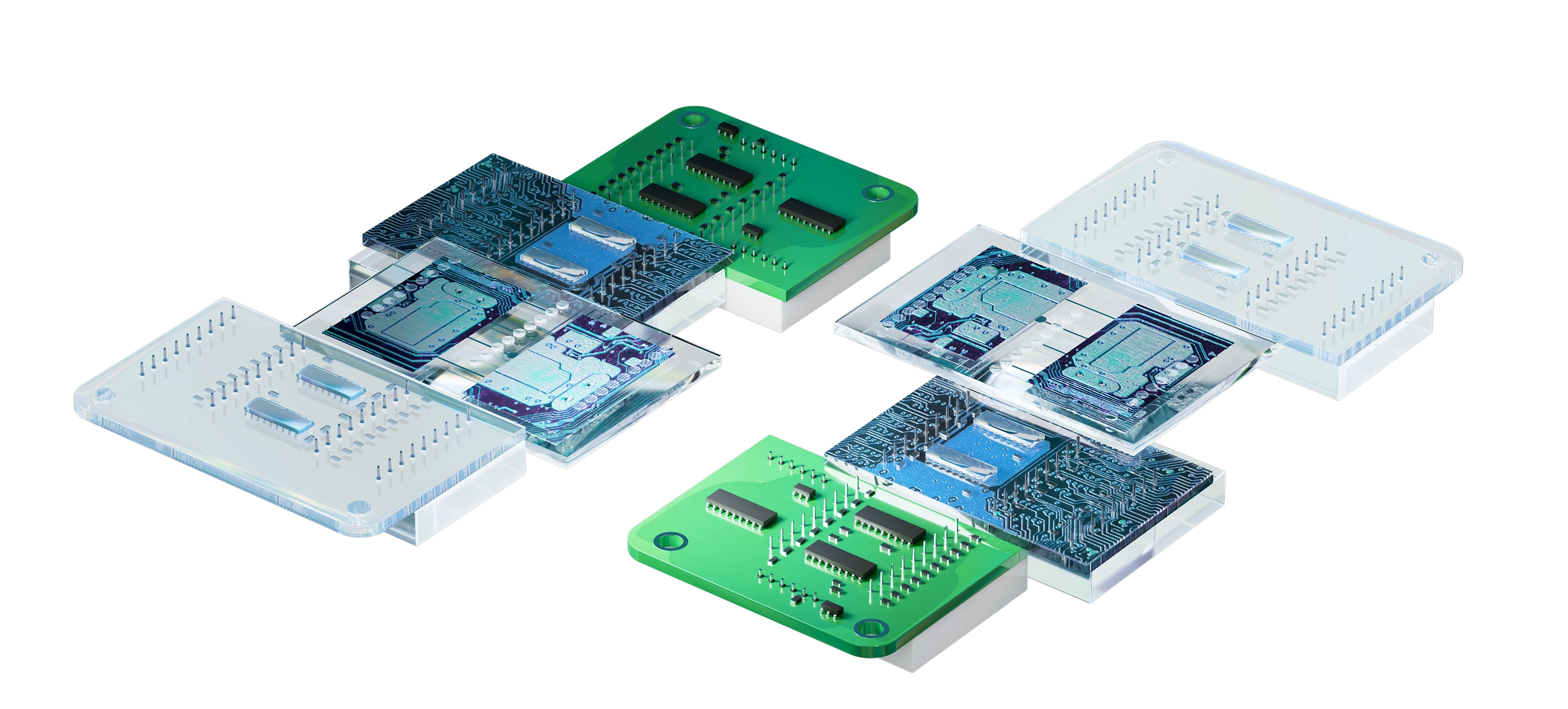
    • Summit can fabricate PCBs ranging from simple 2-layer boards to highly complex designs with 30+ layers as standard, and emerging capabilities extend beyond 44 layers.

    • Standard maximum panel size is 18″ x 24″, with advanced capabilities up to 21″ x 24″ and emerging capabilities reaching 24″ x 36″.

    • Yes, Summit offers HDI layers and sequential laminations from 2-3 up to 7 layers as permitted by laminate type.

    • Summit specializes in advanced PCB technologies including laser micro vias, blind vias, buried vias, and via-in-pad, with options for non-conductive, conductive epoxy, and copper-filled vias.

    • Summit offers HASL (leaded and lead-free), White Tin, ENEPIG, ENIG, Immersion Silver, and Entek Plus HT/OSP finishes for both standard and advanced applications.

    • Yes, Summit provides full turnkey PCB assembly including single and double-sided SMT, through-hole assembly, BGA placement, and additional services like box build, conformal coating, and functional testing.

    • Summit Interconnect maintains comprehensive quality certifications including AS9100D, IPC Class II and III, ITAR registration, and RoHS compliance. Certifications vary by facility based on specialized capabilities.

      View our certifications by facility or contact us to match your project with the right certified location.

    • For inner layers with 1/2 oz. copper, Summit can achieve .003″/.003″ trace width/spacing in advanced capabilities, with emerging capabilities below .0025″/.002″.

    MSIRobot