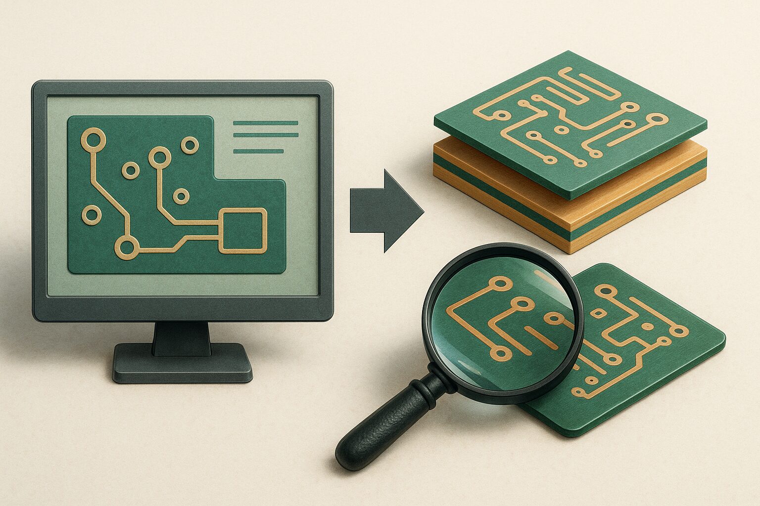
Your connection to advanced PCB manufacturing
 Whenever you route a signal trace, you need to pay attention to the return path for that trace — return signals take the path of least impedance, not the path of least resistance. Ideally, every digital signal line and power rail will have an uninterrupted return path on an adjacent layer. But board layers do not have even spacing, and many designers forget about this fact, especially at the beginning of their career.
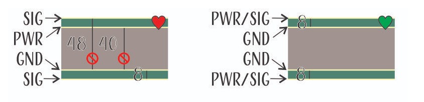
If, for example, you choose to have ground on layer 3 and signal on layer 4, the return path is close, and the field lines will be contained to layers 3 and 4. But, that’s horrible coupling for layers 1 and 2, as they are too far away. Signals on layer 1 will have no choice but to either attempt to pass through layer 2 (which they won’t likely do) or they will simply find a new return path through your power plane, increasing your power rail noise. The power-plane will be far from the ground plane, so the field lines will have ample room to spread and create unwanted noise, and there will be little benefit from capacitive coupling.
A better 4-layer layout has ground on layers 2 and 3 and mixed power/signal on layers 1 and 4. There, the short distance will ensure that the signals are tightly confined to their return paths.
All of that said — as a beginning designer, you should stick to the first, lest preferred option. You’ll have plenty to deal with routing your first project without having to worry about Signal and Power Integrity. Our first design can be made on a solderless breadboard — with the exception of a few components, layout isn’t terribly critical.