

What is a Field?
In physics, a field is a two or three-dimensional region that has a specific and measurable value at every location. It’s not necessary, or even logistically possible, to measure the value at each location, but a measurable value exists at every position.
Vector Fields
While colored arrows make for a visually interesting graphic, it is impossible to do any sort of meaningful math with colors. The magnitude of the acceleration needs a different graphical representation, and the obvious (and perhaps only) answer is to use the length of the arrows to indicate the magnitude of the acceleration,
The question “Is there gravity in the physical space around a single massive object if there are no other objects nearby?” is similar to the question “If a tree falls in the forest and no one is around to hear it, does it make a sound?”
These metaphysical questions make you momentarily stumble because each question takes advantage of innate assumptions about interaction and then removes a necessary second object from the discussion. A better question might be “Does the region of space around a massive object have different object properties than if that massive object wasn’t there?”
The answer is yes – the region of space around the Earth certainly has different properties than if the Earth wasn’t there.
Proof that Mass Alters Space
In Einstein’s Theory of Relativity, massive objects distort space and time.
Einstein’s theories are backed by astronomical observations. Large masses can alter spacetime and warp the path of electromagnetic waves to create a gravitational lens that alters the path of light in a similar way that a galaxy-sized optical lens would.
Einstein also predicted that any information about changes in the location of our imagined object or the position of Earth propagates outwards at the speed of causality (the speed of light 3 x 10⁸(m/s)).
Mass does alter the properties of space-time, and when the mass moves, the information travels outwards at the speed of causality. It takes some amount of time for the changes in the field configuration to propagate outwards.
In September of 2015, scientists confirmed this portion of Einstein’s relativity theory when they detected gravitational waves caused by two colliding black holes.
Physically, there is of course a difference between electromagnetic and gravitational fields. But the underlying mathematics is quite similar.
Electric Fields
“Does the region of space around a charged object have different object properties than if that charged object wasn’t there?” is a more difficult question to answer than the question about mass and acceleration due to gravity.
From the day you were born, you’ve experienced the effects of Earth’s gravity first-hand. But you seldom experience the effects of electrostatic attraction and repulsion.
Electric charge is a mutable object property. Objects might possess a positive charge, a negative charge, or a net-zero charge at any moment as they acquire and lose excess electrons. That makes the behavior of the objects non-uniform: objects sometimes repel; objects sometimes attract; objects sometimes don’t interact at all.
But outside of carefully designed experiments, or when large amounts of electric charge are accidentally stored on your body as you walk across a carpeted floor, there aren’t very many opportunities for you to experience an electric force in your day-to-day life. That means it is difficult to develop intuition about the behavior of charged objects. The closest analog might be playing with magnets.
While you do need two objects to experience a force, you only need one object to perturb a region of space. Mass is an object property that perturbs space in one particular way. Electric charge is an object property that perturbs space in a different way.
The idea that space is altered by the presence of a charge is the basis for the idea of an Electric Field.
Electric fields exist in a region of space around a charged object. The field for a single charged object is given by the equation:
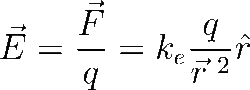
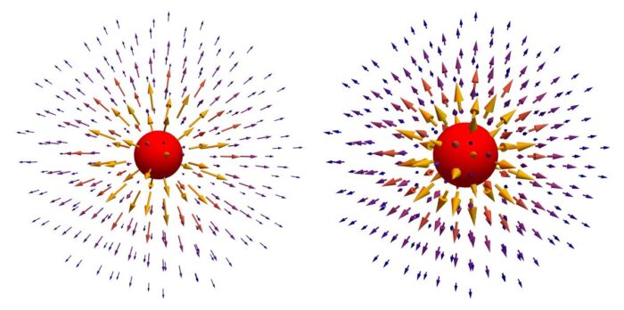
Since there are positive and negative charges, field vectors can point towards or away from the charged object. By convention, vectors point away from positive charges and towards negative charges.
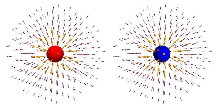
The electric field intensity increases as the charge increases and the electric field intensity decreases as you move further away from an object.
Electric Field Around Multiple Charges
By convention, electric fields start at positive charges and end at negative charges.
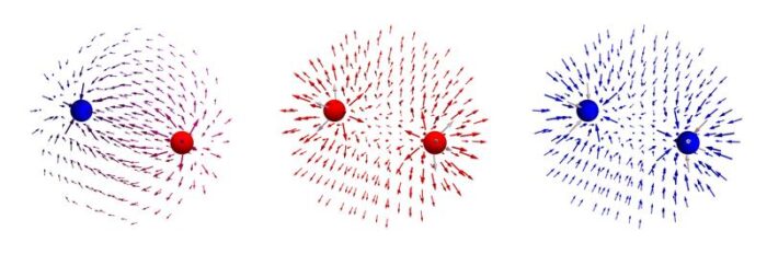
This image shows the three possible charge pair scenarios. On the left, electric field arrows point from positive (red) towards negative (blue). In the middle, the positive charges repel and on the far right, the negative charges repel.
And since drawing all those little arrows can be cumbersome and confusing, it’s far more common to see continuous lines that extend from one charge to another. It is important to remember that these lines do not show the path that charges take from point to point, they are just simplifications of a potentially overwhelming vector field plot.
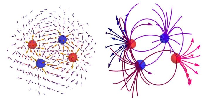
Electric fields are not electric forces. But they establish a mathematical and physical framework in a region of space should additional charges appear. As soon as another charged object is brought into that region of space where the first charged particle exists, the charges will interact and experience a shared force.
Summary
Hopefully, this blog has joggled enough neurons that some of your college physics is rushing back to you. Here are the important points: fields are mathematical models that define the magnitude of a particular object property at all locations in space; changes in the field propagate outwards at a fast, but finite speed; and, field-lines are shortcuts that allow us to avoid drawing an insane number of vectors.
In the next blog in the series, we’ll take a look at charge polarization.
Historically PCB fabrication and delivery of finished products preceded test methods to validate the PCBs. In the 1970’s PCBs were fabricated and shipped without electrical test validation. Mania brought electrical testing to the industry and soon after electrical testing became standard and a requirement for all but the simplest products.
For the next decade PCBs were built by using a “Golden” board programming. The Golden board method used a finished PCB from a finished lot of PCBs and placed on a test fixture, an operator would place the PCB on a tester and initiate a self-learned shorts and opens program from the board. If the second PCB matched the first, a Golden board was established. One of the short comings of the Golden board testing however, is that it is susceptible to missing errors in the supplied fabrication data. The Golden board method would also allow for CAM errors to go undetected up to assembly. The solution finally came when CAM and net compare was made available in the late 1980s. Software was used to validate the received data before fabrication started, the same software was then used to generate an ET program to validate the finished PCB. This method saved product cycle time, prevented the loss of material, and saved manufacturing time at both PCB fabrication and assembly.
The same experience could be said about TDR, and AOI program downloading.
Today the industry is facing the challenge regarding microvia reliability, especially after the reflow of the PCB at assembly, during rework or operating in the field. As with electrical testing in the past, the industry designed PCBs using microvias without evaluating the thermal properties of the material or the geometries in the design. Fabricators produced the finished goods and evaluated the finished PCB to established standards such as IPC-6012. When difficult-to-detect failures occurred post-assembly a test method IPC-TM-650 2.6.27 was established and a caution was added to IPC-6012 rev in section 3.6 Structural Integrity. The testing of a D coupon via IPC-TM-650 2.6.27 did validate that the finished PCBs were safe for assembly, but it did not stop a fabricator from building a bad design. However, until now, there wasn’t a method to simulate a PCB design that validated that the material selection, dielectric thickness, microvia size, and configuration (single, stacked, or staggered microvias) could survive 6x reflows.
As with the evolution of electrical test and the use of the software to validate the design and the final test, we now have software that will validate the structural integrity of a microvia in a design before a PCB stack-up has been approved and implemented into the fabrication process. Our industry now has the opportunity to validate the design, fabricate a microvia design with confidence, and validate that the PCB has met the structural requirements by OM testing to IPC-TM-650 2.6.27.
For more information, listen to Gerry Partida on Altium’s podcast, Design Reliable Multiple Stack Microvias Like a Pro (altium.com).