

When it comes to designing PCBs (Printed Circuit Boards) and ensuring their successful fabrication, an often-overlooked but crucial tool is the impedance table. This table serves as a comprehensive guide that defines all the necessary requirements for your design in an easily accessible format. By providing a well-structured and clear impedance table, you can streamline the fabrication process, reduce questions from your fabricator, and minimize the risk of costly delays.
Understanding Impedance Tables
Before we delve into the tips for creating an impedance table, let’s briefly understand what it is and why it matters.
An impedance table is a document that outlines the essential electrical characteristics and requirements for your PCB design. It typically includes information related to trace width, spacing, dielectric materials, and impedance values for various signal layers. This table serves as a reference point for both designers and fabricators, ensuring that the PCB is manufactured according to the desired electrical specifications.
Why Are Impedance Tables Important?
1. Clarity and Communication: Impedance tables provide a clear and concise reference point for all stakeholders involved in the PCB design and fabrication process. This helps in effective communication between designers and fabricators, reducing the chances of misunderstandings or misinterpretations.
2. Minimizing Errors: By specifying all the necessary requirements in one place, impedance tables minimize the risk of errors during the design and manufacturing phases. This can save time, money, and resources in the long run.
3. Streamlined Fabrication: Fabricators can use the impedance table as a guide to ensure that the finished PCB matches the intended electrical characteristics. This streamlines the fabrication process and reduces the need for time-consuming back-and-forth communication.
Tips for Creating an Effective Impedance Table
Now that we understand the importance of impedance tables, let’s explore some tips for creating an effective one. Following are simple tips and definitions that can help you accurately complete an impedance table:
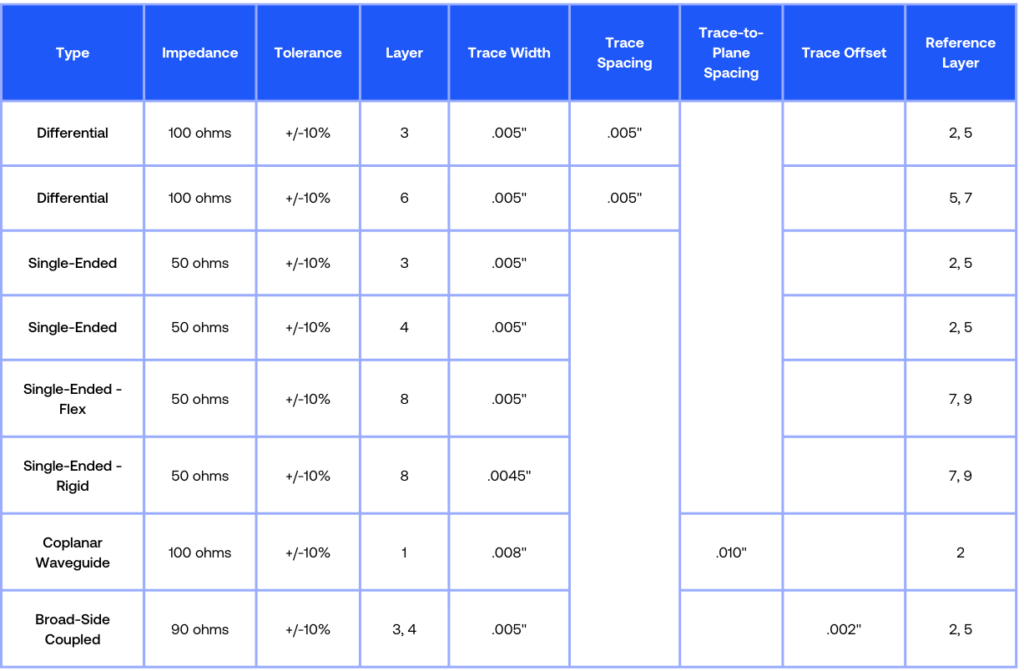
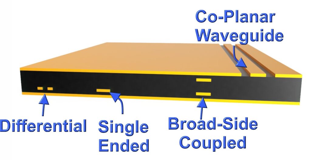
- Type: The impedance type notifies the fabricator what geometry to look for on the layers and what to model on the test coupon.
- Impedance: This column is for the nominal impedance values that are required per trace width, per layer.
- Tolerance: This is the tolerance on the nominal impedance value that will be accepted on the final product.
- Layer: Only the layers that contain the routed impedance traces should be listed on the table. Listing layers where the impedance trace widths aren’t present may delay a job.
- Trace Width: Ensure the trace width listed on the table matches the width that is routed on the design. The impedance traces should not be routed with the same width as the non-impedance-controlled traces.
- Trace Spacing: The trace-to-trace spacing for differential impedance should be listed.
- Trace-to-Plane Spacing: The trace-to-plane spacing for coplanar waveguide impedance should be listed.
- Trace Offset: The offset for broad-side coupled impedance should be listed. Best practice is to route the traces on the same core.
- Reference Layer: This column lists the reference planes in the design that should be modeled in the coupon, per impedance type.
Example Table & Values
The examples below are not exhaustive, and only illustrate some of the common impedance types. For specific impedance questions, please reach out to your sales rep. or our FAE team (summit.fae@summitinterconnect.com) .
Conclusion
In conclusion, impedance tables are indispensable tools for ensuring the successful fabrication of PCB designs. By following the tips outlined in this blog post, you can create an impedance table that is clear, concise, and effective. This will not only help you avoid delays and errors but also enhance communication between you and your fabricator, ultimately leading to a smoother PCB design and manufacturing process.
Summit Interconnect, one of the largest PCB manufacturers in North America, today announced that for the third consecutive year, it has earned a place on Inc. 5000’s prestigious list of America’s Fastest-Growing Private Companies. The list provides a data-driven look at the most successful independent, entrepreneurial businesses.
“Summit is honored to be included on the Inc. 5000 list for the third year in a row,” said Shane Whiteside, president of Summit Interconnect. “To be recognized repeatedly as one of the fastest-growing companies in the country, further confirms we are delivering a best-in-class PCB experience with unmatched service and technical expertise to customers around the world.”
Founded in 2016, Summit Interconnect quickly has become a trusted technology partner and leading manufacturer of high-reliability, advanced technology, printed circuit boards. With an integrated network of eight North American-based facilities, the company continues to expand its PCB services, increase technical support, and add advanced new technology to its facilities.
“Running a business has only gotten harder since the end of the pandemic,” says Inc. editor-in-chief Scott Omelianuk. “To make the Inc. 5000 – with the fast growth that requires – is truly an accomplishment. Inc. is thrilled to honor the companies that are building our future.”
The Inc. 5000 class of 2023 represents companies that have driven rapid revenue growth while navigating inflationary pressure, the rising costs of capital, and seemingly intractable hiring challenges. Among this year’s top 500 companies, the average median three-year revenue growth rate ticked up to an astonishing 2,238 percent. In all, this year’s Inc. 5000 companies have added more than one million jobs to the economy over the past three years.
About Summit Interconnect: Summit Interconnect is the largest, privately held PCB manufacturer in North America. The company is focused on the fast-growing defense and high-performance commercial sectors in the North American market. Summit offers solutions ranging from advanced cutting-edge prototyping to complex high mix, low-to-mid volume production. Summit’s facilities are located across California, Illinois, Colorado, and Toronto, Canada. For more information, please visit summit-pcb.com.
Media Contact: Lisa Holmes, Director of Marketing, Summit Interconnect, 303-307-9909, lisa.holmes@summit-pcb.com.